ASML unlocks next-generation AI chip scaling as High-NA lithography enters mass production
High-NA lithography delivers the transistor density and power efficiency to overcome scaling barriers and fuel global AI innovation.
February 27, 2026
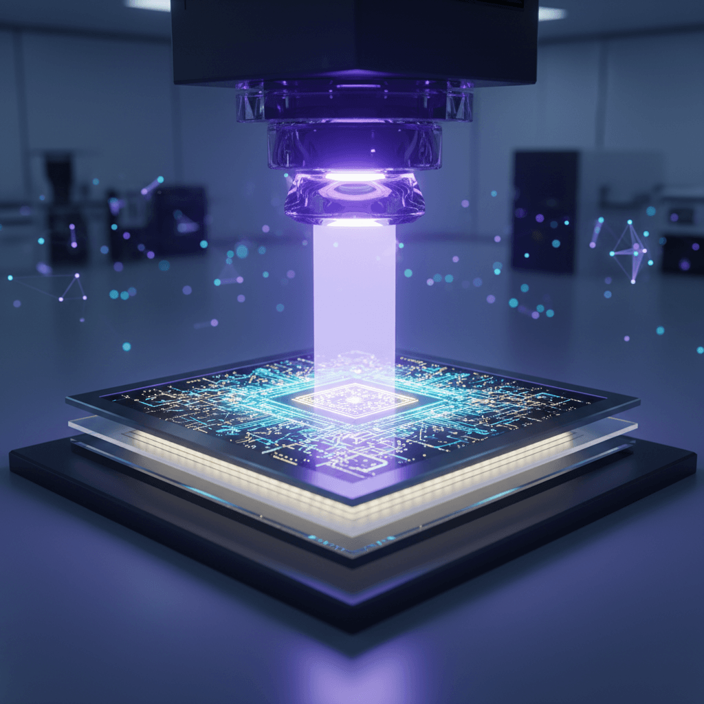
The semiconductor industry has reached a pivotal transition point as the primary technology required to manufacture the next generation of artificial intelligence chips has officially been declared ready for mass production. ASML, the Netherlands-based firm that maintains a global monopoly on the critical lithography equipment used to etch patterns onto silicon, confirmed that its High-Numerical Aperture Extreme Ultraviolet lithography tools have successfully transitioned from the research and development phase to high-volume manufacturing readiness.[1] This development effectively clears the path for a new era of silicon scaling, promising to overcome the physical and economic barriers that have threatened to slow the progress of computing power just as the demand for AI infrastructure reaches an all-time high.
The core of this advancement lies in a fundamental upgrade to the optical systems used in the chipmaking process.[2] Standard extreme ultraviolet systems, which have been the industry workhorse for the past several years, operate with a numerical aperture of 0.33. The new High-NA systems increase this figure to 0.55, a technical shift that significantly sharpens the focus of the light used to print circuit designs.[2][3][4] While both generations utilize a light wavelength of 13.5 nanometers, the higher numerical aperture allows the system to resolve features as small as 8 nanometers, compared to the 13-nanometer limit of the previous generation.[3] This increased resolution enables chipmakers to pack transistors 1.7 times more densely and achieve a nearly threefold increase in transistor density per square millimeter. For the AI industry, where the performance of large language models is often limited by the sheer number of parameters a single chip can process, this leap in density is the essential foundation for the hardware of the next decade.[5]
One of the most significant advantages of the High-NA transition is the simplification of the manufacturing process itself. As transistor sizes have shrunk, chipmakers have been forced to rely on a technique known as multi-patterning, where a single layer of a chip is exposed multiple times to achieve the necessary detail. While effective, multi-patterning is notoriously complex and expensive, increasing the risk of defects and extending the time it takes to move a wafer through the factory. The High-NA tools allow for single-exposure patterning of even the most intricate layers, reducing the total number of manufacturing steps from dozens down to a handful for certain critical components. By eliminating these extra steps, foundries can potentially achieve higher yields and faster production cycles, which are critical metrics for meeting the insatiable demand for AI-grade logic and high-density memory.
The adoption of this technology has sparked a high-stakes strategic divide among the world’s leading chip manufacturers.[5] Intel has emerged as the most aggressive first-mover, having already installed the industry’s first commercial High-NA scanners at its research and development facility in Oregon. The company plans to utilize these tools for its upcoming 14A process node, which is slated for volume production within the next two years.[6][5] By being the first to master the learning curve associated with these machines, Intel aims to reclaim its position as the world leader in process technology, a title it lost to Taiwan Semiconductor Manufacturing Company nearly a decade ago. Intel has already reported successful acceptance testing for its latest scanners, which can process approximately 175 wafers per hour, with plans to eventually push that throughput toward 220 wafers per hour through further software and hardware tuning.
In contrast, TSMC has adopted a more cautious approach, signaling that it may delay the full-scale adoption of High-NA tools until the economics are more favorable.[5] The Taiwanese giant, which currently produces the vast majority of the world’s most advanced AI chips for companies like Nvidia and Apple, has argued that it can continue to achieve the necessary scaling for its near-term roadmaps using existing low-NA equipment combined with advanced multi-patterning techniques. The primary barrier is the astronomical cost of the equipment; a single High-NA scanner is priced at approximately 400 million dollars, nearly double the cost of the previous generation.[1] For foundries operating at the scale of TSMC, the decision to switch requires a delicate balance between the performance benefits of the new optics and the massive capital expenditure required to reconfigure entire factories to accommodate the larger, heavier machines.
Despite the economic friction, the implications for the AI sector are profound and far-reaching. The chips produced via High-NA lithography are expected to deliver substantial improvements in power efficiency, with early estimates suggesting a 25 to 35 percent reduction in power consumption for equivalent performance levels.[5] This is a critical factor for the future of artificial intelligence, as the energy requirements of massive data centers have become a significant bottleneck for the expansion of the industry. As large-scale AI training moves toward models with trillions of parameters, the ability to pack more compute power into a smaller, more energy-efficient footprint becomes the only viable path forward. Furthermore, High-NA technology is not limited to logic chips; it is also being integrated into the production of next-generation high-bandwidth memory, which is essential for the rapid data transfer rates required by AI accelerators.
The transition to High-NA also marks a significant shift in the geopolitical landscape of the semiconductor industry. Because ASML is the sole provider of this technology, and the development of the optics involves a tightly knit ecosystem of European and American partners, the equipment has become a focal point of international trade policies. While the machines are now ready for mass production, their distribution is subject to strict export controls, ensuring that the most advanced manufacturing capabilities remain concentrated within a few specific regions. This has led to a surge in investment in domestic semiconductor manufacturing in the United States and Europe, as governments recognize that the ability to host High-NA-equipped factories is synonymous with having a leading edge in the global AI race.
Integrating these machines into a high-volume manufacturing environment remains a significant engineering challenge. Beyond the lithography tool itself, the entire supporting ecosystem—including photomasks, light-sensitive chemicals known as photoresists, and metrology systems—must be co-optimized to work with the finer resolution of High-NA light.[7][3] ASML has indicated that it is targeting a 90 percent uptime for these systems by the end of the year, a crucial milestone for ensuring that the technology is not just a scientific achievement but a reliable industrial tool. The first 500,000 test wafers have already been processed through these systems, providing a wealth of data that has helped the industry refine the resists and masks needed to minimize defects.
As the semiconductor industry moves into the "angstrom era"—where features are measured in units smaller than a nanometer—the successful deployment of High-NA EUV represents the opening of a new frontier.[8][3] While the costs and technical hurdles are significant, the alternative is a stagnation of Moore's Law that the modern digital economy cannot afford. By clearing the runway for sub-2nm process nodes, ASML and its partners have ensured that the hardware infrastructure will be capable of supporting the next decade of AI innovation. The focus now shifts from the laboratory to the factory floor, where the first commercial chips produced with this technology will soon begin to define the performance limits of the intelligence age.