US Produces First NVIDIA Blackwell AI Wafers, Powering Next-Gen AI
America's semiconductor renaissance begins with AI chip wafers in Arizona, yet critical advanced packaging still awaits US shores.
October 18, 2025
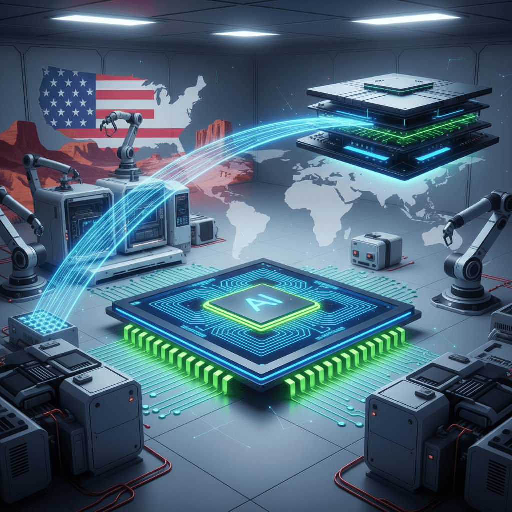
In a landmark achievement for the American technology sector, NVIDIA and Taiwan Semiconductor Manufacturing Company (TSMC) have successfully produced the first production-grade Blackwell architecture wafers on United States soil. The milestone, celebrated at TSMC's burgeoning fabrication plant in Phoenix, Arizona, represents a significant stride in the multi-year effort to revitalize domestic semiconductor manufacturing and secure a critical link in the artificial intelligence supply chain. While the event was hailed as a historic moment, it also casts a bright light on the complex realities and remaining hurdles in the quest for a fully independent, end-to-end American semiconductor ecosystem. The initial wafers, which will serve as the foundation for NVIDIA's next-generation AI and high-performance computing chips, are a tangible result of massive investment and strategic policy aimed at reducing reliance on foreign manufacturing. However, the intricate global supply chain means these cutting-edge silicon discs will still embark on a trans-Pacific journey back to Taiwan for the final, crucial stages of production, underscoring that the vision of a completely US-contained semiconductor pipeline is still on the horizon.
The celebration at the Arizona facility, attended by NVIDIA founder and CEO Jensen Huang, marked the commencement of volume production for one of the most complex pieces of technology in the world.[1][2][3] "It's the very first time in recent American history that the single most important chip is being manufactured here in the United States by the most advanced fab," Huang declared, emphasizing the strategic importance of the achievement.[2][3][4] The Blackwell wafer itself is a marvel of engineering, built on a custom TSMC 4NP process technology and featuring an astounding 208 billion transistors.[5] This architecture is designed to power the next wave of generative AI, offering significant leaps in performance and efficiency.[4] Yet, the production process highlights a critical dependency in the supply chain. After being fabricated in Arizona, the Blackwell wafers must be shipped to Taiwan for advanced packaging using TSMC's sophisticated CoWoS-L (Chip-on-Wafer-on-Substrate with Local Silicon Interconnect) technology.[6] This intricate process is essential for integrating the high-bandwidth memory and other components that allow the Blackwell GPUs to function at their peak, a capability that does not yet exist at scale in the United States.[6][7] This reliance on overseas packaging leaves a strategic vulnerability and adds complexity and cost to the final product.[6]
The establishment of TSMC's Arizona mega-fab is a cornerstone of a broader national strategy, heavily backed by government incentives like the CHIPS and Science Act. TSMC is slated to receive up to $6.6 billion in direct funding and is eligible for up to $5 billion in loans to support its total investment of over $65 billion in its Phoenix facilities.[1][2] This initiative is driven by pressing geopolitical concerns and the vulnerabilities in the global supply chain that were starkly exposed in recent years. For decades, the world has relied heavily on Taiwan for the production of the most advanced semiconductors, creating what is often referred to as the island's "silicon shield."[8] The onshoring of fabrication for chips as critical as NVIDIA's Blackwell is a direct attempt to mitigate the risks associated with this concentration and bolster America's technological leadership and national security.[9][10] TSMC's commitment in Arizona is substantial, with plans for multiple fabs that will eventually produce even more advanced 3-nanometer and 2-nanometer chips, with the company recently announcing it would accelerate its timeline for bringing these next-generation nodes to the US due to strong AI-related demand.[11][12][13][14]
Despite this monumental progress in wafer fabrication, the journey to a self-reliant American semiconductor industry is far from over. The primary obstacle remains the "back-end" of the process: assembly, testing, and, most critically, advanced packaging. North America currently accounts for a mere 3% of the global packaging market, with the vast majority of this highly specialized work concentrated in Asia.[13][15] Rebuilding this domestic capacity is a formidable challenge, requiring not just immense capital investment but also the development of a robust supplier ecosystem and a highly skilled workforce, both of which have diminished over decades of offshoring. Recognizing this gap, the U.S. government has initiated programs like the National Advanced Packaging Manufacturing Program (NAPMP), a $3 billion effort under the CHIPS Act aimed at creating a domestic packaging industry.[9] Private industry is also stepping in, with companies like Amkor announcing plans to build a multi-billion dollar advanced packaging and test facility in Arizona, a move that will complement the wafer production at nearby TSMC.[6][16] However, experts caution that developing these capabilities to the scale and sophistication required will take years of sustained effort and investment.[13][17]
In conclusion, the emergence of the first US-made Blackwell wafer from TSMC's Arizona fab is a powerful symbol of progress in America's semiconductor renaissance. It is a testament to a successful public-private partnership and a significant step toward onshoring the manufacturing of the engines that will power the future of artificial intelligence. Yet, this achievement must be viewed with a clear-eyed understanding of the path that lies ahead. The continued reliance on Taiwan for advanced packaging serves as a crucial reminder that a truly resilient and independent domestic supply chain requires mastery of every stage of production. While the front-end of chipmaking has made a dramatic return to American shores, the long and complex journey to bring the entire semiconductor ecosystem home is still in its early and critical phases, with implications that will shape the global technological landscape for decades to come.
Sources
[2]
[3]
[7]
[11]
[12]
[13]
[14]
[16]
[17]