TCS Launches Chiplet Services, Powering Next-Gen AI Processors
TCS tackles Moore's Law limits with chiplet engineering, fueling AI innovation and strengthening India's semiconductor future.
September 11, 2025
In a strategic move to address the evolving demands of the global semiconductor industry, Tata Consultancy Services (TCS) has launched a suite of chiplet-based system engineering services. This initiative aims to help semiconductor companies innovate beyond the confines of traditional chip design, enabling the development of faster, more powerful, and efficient processors. The launch comes at a critical inflection point for the industry, as the relentless demand for computing power, driven largely by the artificial intelligence boom, pushes against the physical and economic limits of conventional chip manufacturing. By offering specialized expertise in the burgeoning field of chiplets, TCS is positioning itself as a key enabler for the next generation of high-performance computing and strengthening India's ambition to become a significant player in the global semiconductor landscape.[1][2][3]
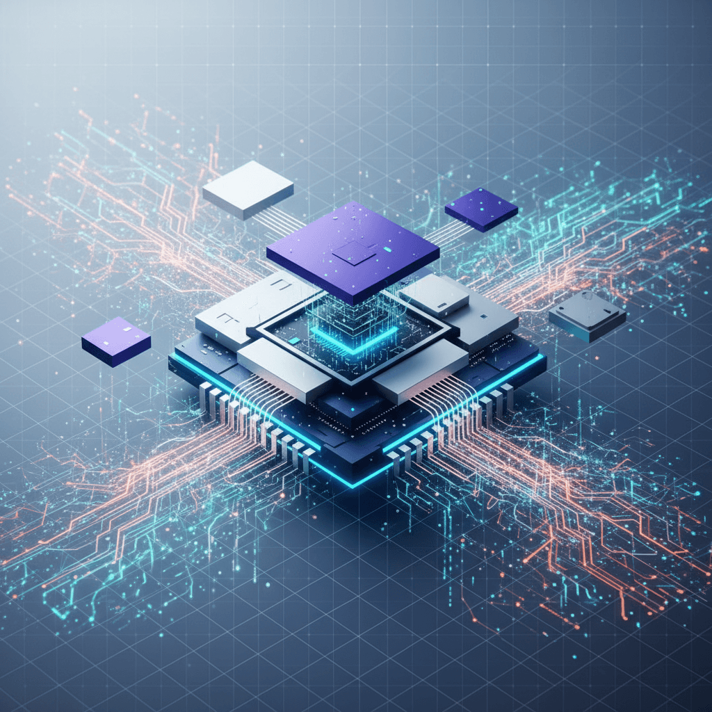
For decades, the semiconductor industry has been guided by Moore's Law, the principle of shrinking transistors to pack more power onto a single, monolithic piece of silicon.[1][3] This approach, however, is facing significant headwinds. As transistors approach atomic scales, further miniaturization is becoming prohibitively complex and expensive, leading to diminishing returns and lower manufacturing yields.[4][5] In response to these challenges, the industry is undergoing a paradigm shift towards chiplet-based design.[1][4][3] This revolutionary approach breaks down a complex, monolithic system-on-chip (SoC) into smaller, specialized functional blocks called chiplets.[6][7][3] These modular chiplets, which can be thought of as technological LEGO bricks, can be developed and manufactured separately—often using different process technologies—and then integrated together in a single package.[8] This modularity offers profound advantages, including enhanced flexibility for designers to mix and match components from various suppliers, reduced development costs, and a significantly faster time-to-market since individual chiplets can be reused across different products.[9][4][10][5]
TCS's new portfolio of services is designed to provide comprehensive support across the entire chiplet ecosystem. The offering includes crucial design and verification services for established industry standards like the Universal Chiplet Interconnect Express (UCIe™) and High Bandwidth Memory (HBM), which are essential for ensuring seamless communication between different chiplets.[1][6][11] Furthermore, TCS is providing advanced package design services, including 2.5D and 3D interposers and multi-layer organic substrates, the critical materials that connect and support these complex multi-chip packages.[1][6][11] This end-to-end "chip-to-system" expertise aims to democratize the design of next-generation chips for a wider range of companies.[1][2] V Rajanna, President of Technology, Software and Services at TCS, stated that the services will help semiconductor enterprises accelerate chiplet tapeout, "driving flexibility, scalability and faster time to market."[1][6][7][3] Leveraging over two decades of experience in the semiconductor sector, TCS has already demonstrated its capability in this domain, citing a recent project with a leading North American firm to simplify the integration of diverse chip types for industry-leading AI processors.[1][2][11]
The implications of this shift to chiplets are particularly profound for the artificial intelligence industry. The massive computational power required for training and running large language models and other sophisticated AI workloads is stretching the capabilities of traditional hardware.[8][12] Chiplet-based architectures are uniquely suited to meet these demands.[9][13] They allow for unprecedented scalability and customization, enabling the creation of bespoke AI accelerators where multiple compute cores, memory interfaces, and other specialized units can be integrated to optimize for specific tasks like natural language processing or computer vision.[9][8] This leads to hardware that is not only more powerful but also more energy-efficient, a critical consideration as the carbon footprint of AI data centers becomes a growing concern.[13][12] By facilitating the development of these customized systems, chiplet technology could challenge the current dominance of general-purpose GPUs in the AI space, paving the way for a new wave of hardware innovation tailored specifically for the age of AI.[14][13]
The timing of TCS's launch is also significant for India's burgeoning semiconductor ambitions.[1][7][3] The Indian government's ₹76,000 crore India Semiconductor Mission is a clear signal of the country's intent to establish itself as a global hub for chip design and manufacturing.[1][15] The nation's semiconductor market, valued between $45 and $50 billion, is projected to more than double to over $100 billion by 2030.[1][3][11] With India already home to 20% of the world's chip design engineers, the ecosystem is primed for growth.[1][16][15] The availability of world-class expertise in advanced chip-to-system engineering from a domestic leader like TCS is expected to significantly strengthen this momentum.[1][7] It provides both Indian and international companies with the critical support needed to navigate the complexities of chiplet integration, thereby accelerating innovation and reinforcing the country's role in the global supply chain.[7]
In conclusion, TCS's foray into chiplet-based engineering services represents a strategic response to a fundamental transformation within the semiconductor world. By embracing the modular, flexible, and cost-effective chiplet model, the company is not only addressing the immediate challenges of scaling traditional chip designs but is also unlocking the potential for the next generation of high-performance computing. This move is poised to have a cascading effect, most notably by fueling the hardware innovation required to sustain the rapid advancement of artificial intelligence. For the global tech landscape, it signals a more democratized and dynamic future for chip design, and for India, it marks a significant step forward in its journey to becoming a self-reliant and influential force in the vital semiconductor industry.