Lithography leader ASML pivots to advanced packaging to break the global AI hardware bottleneck
The lithography giant is expanding into advanced packaging to master the complex 3D integration essential for the AI revolution.
March 2, 2026
For decades, ASML has occupied a unique and unassailable position at the pinnacle of the semiconductor industry. As the world’s sole manufacturer of extreme ultraviolet lithography systems, the Dutch company has been the gatekeeper of progress for the most advanced chips on Earth. These machines, which use light with a wavelength of just 13.5 nanometers to etch billions of transistors onto silicon, are the only tools capable of producing the high-performance processors that power modern smartphones, supercomputers, and the foundational infrastructure of artificial intelligence. However, as the industry begins to approach the physical and economic boundaries of traditional transistor scaling, ASML is signaling a monumental shift in its corporate strategy. The company is now looking beyond the act of printing circuits and moving aggressively into the domain of advanced packaging.[1][2][3][4][5][6][7][8] This pivot represents a recognition that the future of computing performance will no longer be determined solely by how small a single chip can be made, but by how effectively multiple specialized chips can be bonded and connected into a cohesive, high-performance system.
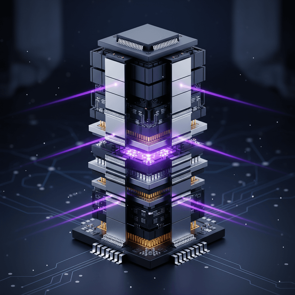
The motivation behind this expansion is rooted in the explosive growth of the artificial intelligence sector. Modern AI models, which require vast amounts of compute power and memory bandwidth, have reached a point where traditional monolithic chip designs are no longer sufficient. To meet these demands, chip designers at companies like Nvidia and AMD have moved away from single, flat silicon dies toward heterogeneous integration.[1] This involves combining various specialized components—such as logic processors, high-bandwidth memory, and connectivity chiplets—into a single package. While packaging was once considered a low-margin, high-volume "back-end" process focused primarily on protecting the silicon and connecting it to a printed circuit board, it has now become a critical "front-end" discipline.[7][1] The precision required to stack these components in three-dimensional "skyscraper" architectures and connect them with nanometer-scale accuracy is now approaching the complexity of the lithography process itself. By entering the advanced packaging market, ASML aims to leverage its unrivaled expertise in optics, precision metrology, and wafer handling to capture a greater share of the value created during these final, high-stakes stages of manufacturing.
ASML’s entry into this space is anchored by the development of specialized hardware designed to bridge the gap between traditional wafer fabrication and the assembly of multi-chip modules.[8] A key component of this new product line is a high-productivity lithography system specifically optimized for the redistribution layers and interconnects required in advanced packaging environments. This system, which recently entered the high-volume manufacturing phase, offers significantly higher throughput and superior overlay accuracy compared to existing solutions in the packaging market. Beyond this specialized scanner, the company is also exploring "holistic lithography" solutions that integrate advanced metrology and inspection tools. These tools utilize electron-beam technology and machine learning algorithms to detect nanometer-scale defects that could compromise the yield of complex 3D-integrated chips. Because a single faulty component in an advanced package can ruin the entire multi-thousand-dollar processor, the demand for extreme precision and high-yield inspection has never been higher. ASML is positioning itself as the only provider capable of offering a seamless transition from the primary patterning of transistors to the intricate interconnecting of those transistors in a finished package.
Another significant frontier in ASML’s expansion involves breaking through the physical limitations of chip size.[4] Currently, the maximum area that a lithography machine can exposure in a single pass is roughly the size of a postage stamp.[6][4][8][5][7] While this was sufficient for most historical applications, the massive scale of next-generation AI accelerators is pushing against this "reticle limit." To accommodate the enormous logic and memory requirements of AI training hardware, manufacturers often must stitch multiple exposures together or find ways to fuse several large dies into a single package.[8] ASML is currently researching ways to expand the maximum field size of its scanners, potentially allowing for the production of larger, more powerful single-die processors. This effort is complemented by the company’s ongoing development of high numerical aperture systems, which provide the resolution needed for the next several generations of transistor nodes. By aligning these front-end advancements with its new packaging initiatives, ASML is creating a dual-track strategy to ensure that the "scissor gap"—the widening distance between compute demand and the pace of traditional scaling—does not become an insurmountable bottleneck for the AI industry.
The strategic shift also follows a transition in ASML’s leadership and a reorganization of its engineering divisions.[6][8][9] The company has moved to prioritize technical roles and engineering excellence in its management structure, signaling a long-term commitment to research and development that extends over the next decade and beyond. This internal alignment is crucial as ASML prepares to compete and collaborate with other semiconductor equipment giants that have historically dominated the packaging and metrology sectors. While companies like Applied Materials and Lam Research have established strong positions in the "back-end" of the industry, ASML’s unique advantage lies in its ability to standardize processes across the entire manufacturing chain. By bringing scanner-level performance to the packaging line, ASML is effectively turning packaging back into a lithography-centric discipline—a field where it has no equal. This move is expected to reshape the supply chain for major foundries and memory makers, who are increasingly looking for integrated solutions to simplify the production of high-bandwidth memory and logic-stacked accelerators.
For the global AI industry, the implications of ASML’s expansion are profound. The bottleneck in AI hardware availability is often not just the number of logic chips being produced, but the capacity and yield of the advanced packaging lines required to assemble them. By introducing more accurate and productive tools into this segment, ASML could significantly improve the reliability and scale of AI chip production, potentially leading to a more consistent supply of the hardware necessary for the next generation of large-scale language models and autonomous systems. Furthermore, as the industry moves toward more complex 3D architectures, the synergy between ASML’s lithography dominance and its new packaging offerings could accelerate the development of chips that are both more energy-efficient and capable of handling higher data throughput. This is essential for the continued evolution of AI applications that require real-time processing and massive memory access.
Ultimately, ASML’s foray into advanced packaging marks the end of an era where lithography was viewed as a standalone stage of the chipmaking process. The company is evolving from a supplier of a single, albeit essential, tool into a comprehensive infrastructure provider for the semiconductor industry’s most difficult challenges. As the boundaries between the front-end and back-end of the line continue to blur, ASML’s 10-to-15-year roadmap suggests a future where the company is as much about the "glue" that holds chips together as it is about the light that prints them.[8][6] This transition ensures that even as the physical limits of the silicon atom are reached, the architectural innovation driving the AI revolution can continue unabated. By controlling the tools that both define and assemble the modern processor, ASML is cementing its role as the indispensable foundation upon which the future of computing will be built.